Reading view

There are new articles available, click to refresh the page.

Cheap 10x10cm Hotplate Punches Above Its Weight

For less than $30 USD, you can get a 10×10 centimeter hotplate with 350 Watts of power. Sounds mighty fine to us, so surely there must be a catch? Maybe not, as [Stefan Nikolaj]’s review of this AliExpress hotplate details, it seems to be just fine enough.

At this price, you’d expect some shoddy electronics inside, or maybe outright fiery design decisions, in the vein of other reviews for similar cheap heat-producing tech that we’ve seen over the years. Nope – the control circuitry seems to be more than well-built for our standards, with isolation and separation where it matters, the input being fused away, and the chassis firmly earthed. [Stefan] highlights just two possible problem areas: a wire nut that could potentially be dodgy, and lack of a thermal fuse. Both can be remedied easily enough after you get one of these, and for the price, it’s a no-brainer. Apart from the review, there’s also general usage recommendations from [Stefan] in the end of the blog post.

While we’re happy to see folks designing their own PCB hotplates or modifying old waffle irons, the availability of cheap turn-key options like this means there’s less of a reason to go the DIY route. Now, if you’re in the market for even more build volume, you can get one of the classic reflow ovens, and maybe do a controller upgrade while you’re at it.

Putting KDE On Raspberry Pi OS Simpler Than Expected

Raspberry Pi boards are no longer constrained – these days, you can get a quad-core board with 8 or 16GB of RAM to go around, equip it with a heatsink, and get a decently comfortable shop/desk/kitchen computer with GPIOs, cameras, speedy networking, maybe even NVMe, and all the wireless you’d expect.

Raspberry OS, however, remains lightweight with its pre-installed LXDE environment – and, in many cases, it feels quite constrained. In case you ever idly wondered about giving your speedy Pi a better UI, [Luc]/[lucstechblog] wants to remind you that setting up KDE on your Raspberry OS install is dead simple and requires only about a dozen commandline steps.

[Luc] walks you through these dozen steps, from installation to switching the default DE, and the few hangups you might expect after the switch; if you want to free up some disk space afterwards, [Luc] shows how to get rid of the original LXDE packages. Got the latest Trixie-based Pi OS? There’s an update post detailing the few necessary changes, as well as talking about others’ experiences with the switch.

All in all, [Luc] demonstrates that KDE will have a fair bit of graphical and UX advantages, while operating only a little slower, and if you weren’t really using your powerful Pi to the fullest, it’s a worthwhile visual and usability upgrade. For the regular desktop users, KDE has recently released their own distro, and our own [Jenny] has taken a look at it.

Super Simple Deadbuggable Bluetooth Chip

We’re all used to Bluetooth chips coming in QFN and BGA formats, at a minimum of 30-40 pins, sometimes even a hundred. What about ten pins, with 1.27 mm pitch? [deqing] from Hackaday.io shows us a chip from WCH, CH571K, in what’s essentially a SO-10 package (ESSOP10). This chip has a RISC-V core, requires only three components to run, and can work Bluetooth through a simple wire antenna.

This chip is a RISC-V MCU with a Bluetooth peripheral built in, and comes from the CH57x family of WCH chips that resemble the nRF series we’re all used to. You get a fair few peripherals: UART, SPI, and ADC, and of course, Bluetooth 4 with Low Energy support to communicate with a smart device of your choice. For extra hacker cred, [deqing] deadbugs it, gluing all components and a 2.54 mm header for FTDI comms onto the chip, and shows us a demo using webBluetooth to toggle an LED through a button in the browser.

You need not be afraid of SDKs with this one. There’s Arduino IDE support (currently done through a fork of arduino_core_ch32) and a fair few external tools, including at least two programming tools, one official and one third-party. The chip is under a dollar on LCSC, even less if you buy multiple, so it’s worth throwing a few into your shopping cart. What could you do with it once received? Well, you could retrofit your smoke alarms with Bluetooth, create your own tire pressure monitors, or just build a smartphone-connected business card!

PCB Design Review: TinySparrow, A Module For CAN Hacking, v2

A year ago, I’ve design reviewed an MCU module for CAN hacking, called TinySparrow. Modules are plenty cool, and even more so when they’re intended for remaking car ECUs. For a while now, every car has heavily depended on a computer to control the operation of everything inside it – the engine and its infrastructure, the lights, and  Sadly, ECUs are quite non-hackable, so building your own ECUs only makes sense – which is why it’s heartwarming to see modules intended to make this easier on the budding ECU designer!

Last time we saw this module, it was quite a bit simpler. We talked about fixing a number of things – the linear regulator, the unprotected CAN transceiver, and the pinout; we also made the board cheaper to produce by reducing the layer count and instead pushing the clearance/track width limits. This time, we’re seeing TinySparrow v2 , redesigned accounting for the feedback and upgraded with a new MCU – it’s quite a bit more powerful!

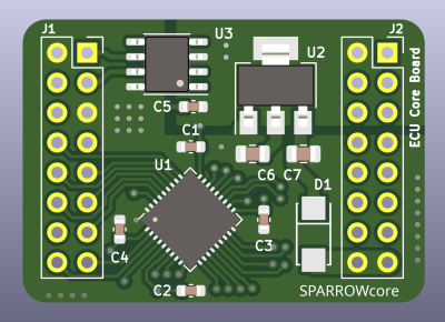
For a start, it’s got ESD diodes, a switching-linear regulator chain for clean but efficient power supply, and most importantly, an upgraded MCU, now with USB and one more CAN channel for a total of two! There’s a lot more GPIOs to go around, too, so the PCB now uses all four of its sides for breakout out power, programming, and GPIO pads. Only a tiny bit bigger than its v1, this module packs a fair bit of punch.

Let’s revisit the design, and try to find anything still left to improve – there’s a few noteworthy things I found.

Protection Almost Perfect

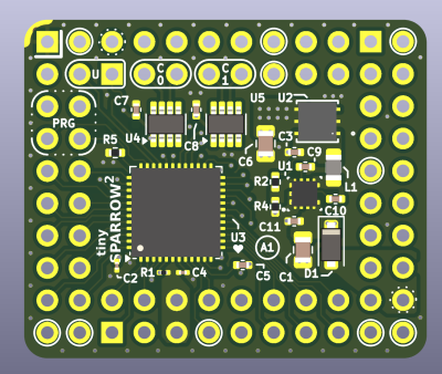
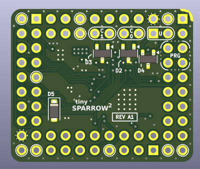
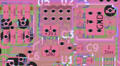
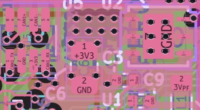
It took me a bit to try and find the ESD diodes mentioned in the README – I didn’t notice that they’re basically the only thing on the bottom layer. This is fine – protection elements like ESD diodes can be on a different layer, and as they’re SOT-23, they’re easy to solder on post-factum. This is quite a nice placement choice, in my opinion – you can basically solder this board with cheaper single-side assembly, use ESD-less boards for your bench testing, and then simply solder the few bottom side components onto “production” versions!

There is but one hiccup with the way they’re placed. ESD diode appnotes will tell you – there’s some extra considerations you can try and put into ESD diode layout. This design pulls connector tracks directly to the CAN ICs on top layer, and directly to diodes on the bottom one. Instead, you should try and route the signal “through” the ESD diodes – letting track inductance play in your favour, and not impeding the ESD diode’s impact.

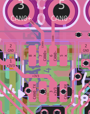
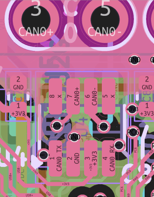
Fortunately, by lightly rerouting 3.3V CAN transceiver power inputs and a few surrounding signals, we can put CAN+ and CAN- signals through vias under the package, so that the signal flows “in series” with ESD diode pads. Similarly, the ESD diodes get vias to ground, shared with transceiver ground vias, but oh well. It’s not perfect, but to my eye, it’s better than before, as far as ESD protection is concerned.

About the only problem I can see with the reroute, is having to reshuffle USB signals, putting them closer together. However, as long as they’re intra-pair length-matched, they’ll do just fine.

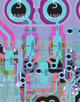
Vias Fit Inside Pads, But Maybe Don’t?

This is not the only change to consider as far as signal routing goes, but it’s the most major one. The next issue I see, is vias – specifically, vias inside component pads.

I’ve had a few run-ins with via-in-pad related problems. Previously, I’ve failed to assemble some boards specifically because of via-in-pad related problems, with solder paste wicking through the board and onto the opposite side. For 0402 components I used, this made a number of boards essentially non-solderable depending on how lucky I got reflowing them, and I had to run a new board revision to get the yield up.

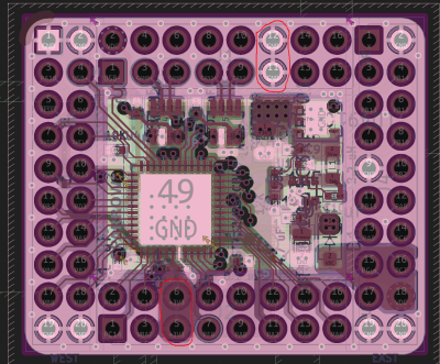
This board’s files have a fair few hints about getting assembled by JLCPCB, and JLC can definitely do plugged vias, preventing any sorts of solder flowing through the board. If the designer or someone else takes the board elsewhere, however, that might no longer apply, which would be disappointing. Also, you might have to pay extra for plugging holes – just like with the previous review, let’s see if we can avoid it. Most problematic areas are around the transceivers, still – especially given the board files now have a custom rule for 0.5mm via-to-via distances. This is not a constraint I’ve seen actually stressed by JLCPCB, but I don’t mind – with just a little bit more signal shuffling, every newly moved via landed within the 0.5mm target area.

Pinout Considerations, Again

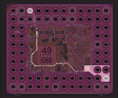
The VDC pin now has GND pins to match, and in general, there’s a lot more GND pins to go around – which is great! It’s pretty surprising to me that the VDC pin is duplicated and its trace goes across the board on an inner layer. This is supposed to be an at least somewhat unfiltered and unprotected car power rail, after all, and I don’t think that’d help things like noise integrity. Maybe this helps with testing because all the core signals are brought to the same corner, but to my eye, it has bad vibes.

The module could perhaps use a key pin – there’s zero omissions in the outer dual-row, which leaves for a possibility of inserting this module rotated 180 degrees by accident, likely obliterating at least something on the module. If these modules are ever meant to be swapped during testing, i.e. using machined headers, I’d try and remove one of the pins from the equation – there’s a NC pin in one of the corners already, thankfully.

There’s a pair of 3.3 V signals and GND signals on the opposite sides of each other. This is geometrically satisfying pinout-wise, and, it would short-circuit the module’s onboard regulator if the module’s ever rotated inserted 180 degrees. This is generally harmless with modern modules, but it could very well make the switching or the linear regulator heat up to finger-burning temperatures – last thing you need when trying to remove a module inserted incorrectly!

Thankfully, at the top, there’s a few unconnected pads, so perhaps GND and NC could swap places, making sure that 3.3 V lands on NC once rotated 180 degrees. The VDC pads could perhaps use the same consideration, but I’m comfortable leaving those as homework.

Moving Forward

It’s a joy to see how much the TinySparrow module has grown in its v2. From vastly improved layout to higher consideration given to design rules, nicer silkscreen, and a way more powerful MCU while at it, it’s that much more of a viable heart for a somewhat modern car, and it’d be quite nice to see some boards utilizing it in the future. I hope this review can help!

As usual, if you would like a design review for your board, submit a tip to us with [design review] in the title, linking to your board files. KiCad design files strongly preferred, both repository-stored files (GitHub/GitLab/etc) and shady Google Drive/Dropbox/etc .zip links are accepted.

RP2350 Done Framework Style

Ever want a microcontroller addon for your laptops? You could do worse than match one of the new and powerful microcontrollers on the block to one of the most addon-friendly laptops, in the way the Framework RP2350 laptop card does it. Plug it in, and you get a heap of USB-connected IO coming out of the side of your laptop – what’s not to love?

The card utilizes the Framework module board space to the fullest extent possible, leaving IO expansion on SMD pads you could marry to a male or female header, your choice. With about seventeen GPIOs, power, and ground, there’s really no limit on what you could add to the side connector – maybe it’d be a logic analyzer buffer, or a breadboard cable, or a flash chip reader, maybe, even an addon to turn it into a pirate version of a Bus Pirate? There’s a fair few RP2350 peripherals available on the side header GPIOs, so sky’s the limit.

Naturally, the card is fully open-source, and even has two versions with two different USB-C plug connectors, we guess, depending on which one is better liked by your PCBA process. Want one? Just send off the files! Last time we saw an addon adding GPIOs to your laptop, it was a Pi Zero put into the optical bay of a Thinkpad, also with an expansion header available on the side – pairing yet another legendary board with a legendary laptop.

One Lucky 3DS Gets A Switch-Style Dock

The Nintendo Switch dock set a new bar for handheld docking user experience – just plug your console in to charge it, output image to your monitor, and keep it working with any USB peripherals of your choice. What if a 3DS is more your jam? [KOUZEX] shows off a Switch-style dock design for his gorgeous yellow 3DS, with Switch Pro controller support, and this dock wasn’t just a 3D printing job – there’s a fair bit of electronics to show, too.

While the 3DS looks stock at a glance, it has already been upgraded internally – there’s a USB-C capture card built in, half-ticking the “monitor output” requirement, and a Raspberry Pi board turns that output into HDMI. Building a charging dock is also pretty simple, with just two contacts on the side that desire 5V. Now, the pro controller support was a fair bit harder – requiring an internal modchip for emulating buttons, and trying out receiver boards for the Switch controller until a well-functioning one was found.

The build video is quite satisfying to watch, from assembling some QFNs onto tiny OSHPark boards using a hotplate and soldering them into the 3DS, to planning out, building, and dremeling some prints to create a true slide-console-into-dock experience, same way the Switch pulled it off. It even has the same USB-C and HDMI arrangement as the Switch dock, too! Want a simpler dock for your 3DS? Don’t forget that you can build a charger dock for yours with just a 3D print and a few wires.

Cheap And Aggressive DRAM Chip Tester

People enjoy retrocomputing for a wide variety of reasons – sometimes it’s about having a computer you could fully learn, or nostalgia for chips that played a part in your childhood. There’s definitely some credit to give for the fuzzy feeling you get booting up a computer you built out of chips. Old technology does deteriorate fast, however, and RAM chip failures are especially frustrating. What if you got a few hundred DRAM chips to go through? Here’s a DRAM chip tester by [Andreas]/[tops4u] – optimized for scanning speed, useful for computers like the ZX Spectrum or Oric, and built around an ATMega328P, which you surely still have in one of your drawers.

The tester is aimed at DIP16/18/20 and ZIP style DRAM chips – [Andreas] claims support for 4164, 41256, 6416, 6464, 514256, and 44100 series RAM chips. The tester is extremely easy to operate, cheap to build, ruthlessly optimized for testing speed, sports a low footprint, and is fully open-source. If you’re ever stuck with a heap of RAM chips you want to quickly test one by one, putting together one of these testers is definitely the path to take, instead of trying to boot up your well-aged machine with a bunch of chips that’d take a while to test or, at worst, could even fry it.

[Andreas] includes KiCad PCB and Arduino source files, all under GPL. They also provide adapter PCBs for chips like the 4116. What’s more, there are PCB files to build this tester in full DIP, in case that’s more your style! It’s far from the first chip tester in the scene, of course, there are quite a few to go around, including some seriously featureful units that even work in-circuit. Not only will they save you from chips that failed, but they’ll also alert you to fake chips that are oh so easy to accidentally buy online!

Standalone USB-PD Stack For All Your Sink Needs

USB PD is a fun protocol to explore, but it can be a bit complex to fully implement. It makes sense we’re seeing new stacks pop up all the time, and today’s stack is a cool one as far as code reusability goes. [Vitaly] over on Hackaday.io brings us pdsink – a C++ based PD stack with no platform dependencies, and fully-featured sink capabilities.

This stack can do SPR (5/9/15/20V) just like you’d expect, but it also does PPS without breaking a sweat – perfect for your Lithium Ion battery charging or any other current-limited shenanigans. What’s more, it can do EPR (28V and up) – for all your high-power needs. For reference, the SPR/PPS/EPR combination is all you could need from a PD stack intended for fully taking advantage of any USB-PD charger’s capabilities. The stack is currently tailored to the classic FUSB302, but [Vitaly] says it wouldn’t be hard to add support for a PD PHY chip of your choice.

It’s nice to have a choice in how you want your PD interactions to go – we’ve covered a few stacks before, and each of them has strong and weak sides. Now, if you have the CPU bandwidth, you could go seriously low-tech and talk PD with just a few resistors, transistors, and GPIOs! Need to debug a particular USB-C edge case? Don’t forget a logger.

UEFI On ARM? More Likely Than You Think

Now, Rock 5 ITX+ is no x86 board, sporting an ARM Rockship RK3588 on its ITX form-factor PCB, but reading this blog post’s headline might as well give you the impression. [Venn] from the [interfacinglinux.com] blog tells us about their journey bringing up UEFI on this board, thanks to the [EDK2-RK3588] project. Why? UEFI is genuinely nice for things like OS switching or system reconfiguration on the fly, and in many aspects, having a system management/configuration interface for your SBC sure beats the “flash microSD card and pray” traditional approach.

In theory, a UEFI binary runs like any other firmware. In theory. For [Venn], the journey wasn’t as smooth, which made it very well worth documenting. There’s maybe not a mountain, but at least a small hill of caveats: having to use a specific HDMI port to see the configuration output, somehow having to flash it onto SPI flash chip specifically (and managing to do that through Gnome file manager of all things), requiring a new enough kernel for GPU hardware acceleration… Yet, it works, it really does.

Worth it? From the looks of it, absolutely. One thing [Venn] points out is, the RK3588 is getting a lot of its features upstreamed, so it’s aiming to become a healthy chip for many a Linux goal. From the blog post comments, we’ve also learned that there’s a RPi UEFI port, even if for a specific CPU revision of the Model 5B, it’s still a nifty thing to know. Want to learn more about UEFI? You can start here or here, and if you want a fun hands-on example, you could very well start by running DOOM.

Build Your Own Glasshole Detector

Connected devices are ubiquitous in our era of wireless chips heavily relying on streaming data to someone else’s servers. This sentence might already start to sound dodgy, and it doesn’t get better when you think about today’s smart glasses, like the ones built by Meta (aka Facebook).

[sh4d0wm45k] doesn’t shy away from fighting fire with fire, and shows you how to build a wireless device detecting Meta’s smart glasses – or any other company’s Bluetooth devices, really, as long as you can match them by the beginning of the Bluetooth MAC address.

[sh4d0wm45k]’s device is a mini light-up sign saying “GLASSHOLE”, that turns bright white as soon as a pair of Meta glasses is detected in the vicinity. Under the hood, a commonly found ESP32 devboard suffices for the task, coupled to two lines of white LEDs on a custom PCB. The code is super simple, sifting through packets flying through the air, and lets you easily contribute with your own OUIs (Organizationally Unique Identifier, first three bytes of a MAC address). It wouldn’t be hard to add such a feature to any device of your own with Arduino code under its hood, or to rewrite it to fit a platform of your choice.

We’ve been talking about smart glasses ever since Google Glass, but recently, with Meta’s offerings, the smart glasses debate has reignited. Due to inherent anti-social aspects of the technology, we can see what’d motivate one to build such a hack. Perhaps, the next thing we’ll see is some sort of spoofed packets shutting off the glasses, making them temporarily inoperable in your presence in a similar way we’ve seen with spamming proximity pairing packets onto iPhones.

❌