❌

Reading view

There are new articles available, click to refresh the page.

Heater is Either a Miracle or a Scam

[Big Clive] picked up a tiny heater for less than Β£8 from the usual sources. Would you be shocked to learn that its heating capacity wasn’t as advertised? No, we weren’t either. But [Clive] treats us to his usual fun teardown and analysis in the video below.

A simple test shows that the heater drew about 800 W for a moment and drops as it heats until it stabilizes at about 300 W. Despite that, these units are often touted as 800 W heaters with claims of heating up an entire house in minutes. Inside are a fan, a ceramic heater, and two PCBs.

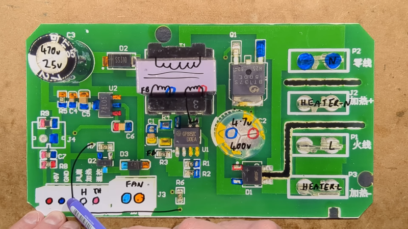
The ceramic heaters are dwarfed by metal fins used as a heat exchanger. The display uses a clever series of touch sensors to save money on switches. The other board is what actually does the work.

[Clive] was, overall, impressed with the PCB. A triac runs the heaters and the fan. It also includes a thermistor for reading the temperature.

You can learn more about the power supply and how the heater measures up in the video. Suffice it to say, that a cheap heater acts like a cheap heater, although as cheap heaters go, this one is built well enough.

Unusual Circuits in the Intel 386’s Standard Cell Logic

Intel’s 386 CPU is notable for being its first x86 CPU to use so-called standard cell logic, which swapped the taping out of individual transistors with wiring up standardized functional blocks. This way you only have to define specific gate types, latches and so on, after which a description of these blocks can be parsed and assembled by a computer into elements of a functioning application-specific integrated circuit (ASIC). This is standard procedure today with register-transfer level (RTL) descriptions being placed and routed for either an FPGA or ASIC target.

That said, [Ken Shirriff] found a few surprises in the 386’s die, some of which threw him for a loop. An intrinsic part of standard cells is that they’re arranged in rows and columns, with data channels between them where signal paths can be routed. The surprise here was finding a stray PMOS transistor right in the midst of one such data channel, which [Ken] speculates is a bug fix for one of the multiplexers. Back then regenerating the layout would have been rather expensive, so a manual fix like this would have made perfect sense. Consider it a bodge wire for ASICs.

Another oddity was an inverter that wasn’t an inverter, which turned out to be just two separate NMOS and PMOS transistors that looked to be wired up as an inverter, but seemed to actually there as part of a multiplexer. As it turns out, it’s hard to determine sometimes whether transistors are connected in these die teardowns, or whether there’s a gap between them, or just an artifact of the light or the etching process.

❌